logo
Dayoo Advanced Ceramic Co.,Ltd
Products
Products
Home > Products > Silicon Carbide Ceramics > Diamond-Shaped Hollow Silicon Carbide Ceramic Wafer Carrier with High Thermal Conductivity and 1400℃ High-temperature Resistance for Semiconductor Applications

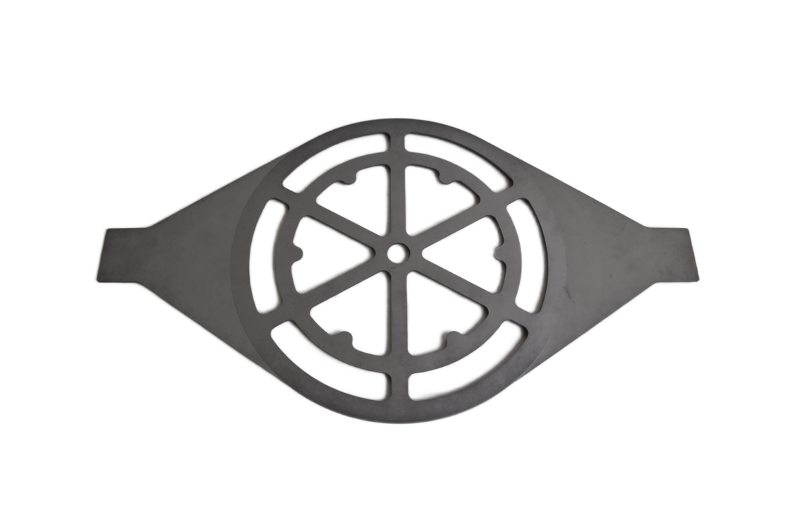
Diamond-Shaped Hollow Silicon Carbide Ceramic Wafer Carrier with High Thermal Conductivity and 1400℃ High-temperature Resistance for Semiconductor Applications

Product Details

Place of Origin: CN

Brand Name: Dayoo

Payment & Shipping Terms

Minimum Order Quantity: Customized

Price: CNY

Packaging Details: package

Delivery Time: 60 workdays

Supply Ability: Factory

Get Best Price
Highlight:
High Thermal Conductivity:
Yes
Thermal Shock Resistance:
Good
Maximum Temperature:
1380℃
Bending Strength:
280 MPa
Purity:
98%
Compressive Strength:
> 2 GPa
High Thermal Conductivity:
Yes
Thermal Shock Resistance:
Good
Maximum Temperature:
1380℃
Bending Strength:
280 MPa
Purity:
98%
Compressive Strength:
> 2 GPa
Diamond-Shaped Hollow Silicon Carbide Ceramic Wafer Carrier with High Thermal Conductivity and 1400℃ High-temperature Resistance for Semiconductor Applications

Diamond-shaped Hollow Silicon Carbide Ceramic Wafer Carrier | Precision Hollow SiC Ceramic Support Plate

Product Introduction

This product is a Diamond-shaped Hollow Silicon Carbide Ceramic Wafer Carrier, manufactured from high-purity silicon carbide (SiC) ceramic raw materials. It features an overall diamond outline with multi-layer annular radial hollow structure in the center. Fabricated via atmospheric pressure high-temperature sintering and precision machining, it boasts high density, lightweight structure and excellent thermal conductivity. The hollow design effectively reduces self-weight and improves gas circulation. It serves as a core load-bearing ceramic component for high-temperature process equipment.

Applications

Widely adopted in semiconductor wafer heat treatment, photovoltaic silicon wafer sintering, optical component annealing, vacuum high-temperature furnaces and other equipment. It works as wafer carrier, airflow baffle and high-temperature fixture, supporting workpieces while ensuring uniform airflow and temperature distribution inside furnaces.

Core Advantages

  • Outstanding High-temperature Resistance: Continuous working temperature up to 1400℃, stable dimension under high temperature.
  • Balanced Thermal Conductivity & Great Thermal Stability: High thermal conductivity and superior thermal shock resistance, resistant to cracking under repeated heating and cooling cycles.
  • High Purity & Contamination-free: Low impurity precipitation, preventing contamination on wafers and precision components.
  • Lightweight Hollow Structure: Reduces weight and optimizes air circulation for faster heating and cooling.

Specification Parameters

表格
Item Parameter
Material Pressureless Sintered Silicon Carbide (SiC) Ceramic
Density ≥3.10g/cm³
Bending Strength ≥350MPa
Continuous Operating Temperature ≤1400℃
Dimensional Tolerance ±0.02mm
Porosity <0.5%

Production Process

Raw Material Mixing & Granulation → Irregular Shape Dry Press Forming → High-temperature Sintering → Surface Precision Grinding → CNC Hollow Milling → Surface Polishing → Ultrasonic Cleaning → Full Dimensional Inspection → Vacuum Packaging

Instructions for Use

  1. Fully bake the carrier before first use to remove adsorbed impurities.
  2. Handle gently when placing workpieces to avoid impact on edges and corners.
  3. Control heating & cooling rate to minimize severe thermal shock.
  4. Regularly clean sediment inside hollow slots to maintain smooth airflow.

After-sales Service

Customization of hollow patterns and overall dimensions based on drawings or samples, prototype trial service available. All products undergo full inspection before delivery with inspection reports provided. After-sales solution for non-artificial quality defects. Professional technical support for high-temperature working condition selection.

FAQ

Q: What are the advantages of SiC carrier compared with alumina ceramic carrier?
 
A: Silicon carbide performs better in high-temperature resistance, thermal conductivity and thermal shock resistance, which is more suitable for heat treatment processes with sustained high temperature and frequent thermal cycles.
 
Q: Can hollow pattern and outer dimension be modified?
 
A: Yes. Outer profile, hollow layout and plate thickness can be adjusted according to workpiece size.